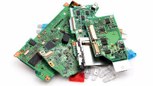
Printed circuit boards are found in nearly any and every electronics product that you can think of, no matter how complex. From your mobile device to your garage door opener, printed circuit boards (PCBs) are the core of the means by which we are able to enjoy the conveniences of today’s technology.
 Of course, electronic devices are used for much more than convenience. Printed circuit boards are also found in medical devices, computerized industrial machinery, modes of transportation, and many, many more areas. Without printed circuit boards, most of the world around us would be very different.Although printed circuit boards have been around for well over 100 years, they — and the possibilities they offer — continue to evolve. As materials and technologies change, PCBs are still getting smaller, even as they’re able to do much more. While it’s often hard to believe what today’s technology is capable of, the truth is that it’s based on a fairly simple concept: electrical conductivity between electrical components. Let’s look at the PCB manufacturing process, which is similar for both prototypes and production PCBs.
Printed circuit boards are found in nearly any and every electronics product that you can think of, no matter how complex. From your mobile device to your garage door opener, printed circuit boards (PCBs) are the core of the means by which we are able to enjoy the conveniences of today’s technology.
Of course, electronic devices are used for much more than convenience. Printed circuit boards are also found in medical devices, computerized industrial machinery, modes of transportation, and many, many more areas. Without printed circuit boards, most of the world around us would be very different.The PCB Manufacturing Process
Create the substrate.
- The “substrate,” or base layer, of a printed circuit board is created from rolled glass fiber lined with a copper foil layer. Glass fiber (and similar materials) won’t interfere with the operation of the PCB, but are able to be effectively plated and have components mounted on them (more on this shortly).
The “substrate,” or base layer, of a printed circuit board is created from rolled glass fiber lined with a copper foil layer. Glass fiber (and similar materials) won’t interfere with the operation of the PCB, but are able to be effectively plated and have components mounted on them (more on this shortly).
Prepare the substrate.
- Once the PCB manufacturing process begins, the substrate must be prepared for the application and assembly of its components and conductors. Depending on the complexity and design of the printed circuit board, this usually involves drilling numerous holes — some which may be conductively plated, and some not. The purpose of these holes could be to allow connections between different sides of the board, different board layers, or for mounting components (on “through-hole mounted” boards — again, more on these terms later).
Once the PCB manufacturing process begins, the substrate must be prepared for the application and assembly of its components and conductors. Depending on the complexity and design of the printed circuit board, this usually involves drilling numerous holes — some which may be conductively plated, and some not. The purpose of these holes could be to allow connections between different sides of the board, different board layers, or for mounting components (on “through-hole mounted” boards — again, more on these terms later).
Create the pattern.
- Before components are added, the PCB pattern must be created on the copper foil surface of the substrate. In this step, a UV light-sensitive material is first affixed to the entire surface of the substrate. A stencil in the intended pattern of the PCB is then laid on top of the substrate, which is then exposed to UV light to “activate” the light-sensitive material. This material becomes soluble and is then easily dissolved, revealing the copper foil in the intended PCB pattern. From here, a thin additional layer of copper is electroplated onto the exposed copper foil, and is then covered with a protective tin coating. Afterward, the remaining, unprotected copper foil is removed.
Before components are added, the PCB pattern must be created on the copper foil surface of the substrate. In this step, a UV light-sensitive material is first affixed to the entire surface of the substrate. A stencil in the intended pattern of the PCB is then laid on top of the substrate, which is then exposed to UV light to “activate” the light-sensitive material. This material becomes soluble and is then easily dissolved, revealing the copper foil in the intended PCB pattern. From here, a thin additional layer of copper is electroplated onto the exposed copper foil, and is then covered with a protective tin coating. Afterward, the remaining, unprotected copper foil is removed.
Intermediate steps.
- Before attaching or mounting the electronic components, a few intermediate preparatory processes are necessary. Contacts are added at the edges of the PCB pattern, and the protective tin coating is removed from the copper plating. The board is also temporarily sealed with epoxy so that the pattern is not damaged during the assembly process.
Before attaching or mounting the electronic components, a few intermediate preparatory processes are necessary. Contacts are added at the edges of the PCB pattern, and the protective tin coating is removed from the copper plating. The board is also temporarily sealed with epoxy so that the pattern is not damaged during the assembly process.
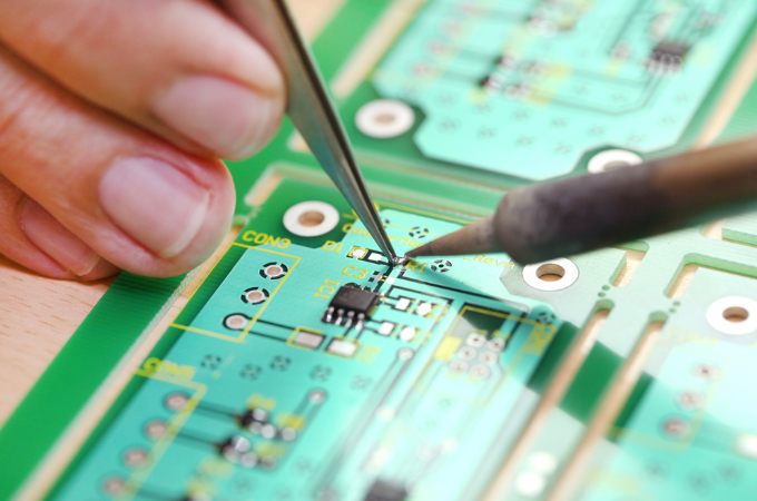
Mounting components.
- Electronic components (e.g., microchips) are attached, or mounted, to the PCB in one of two ways: In a surface-mounting process, the components are soldered right to the board, in direct contact with the circuit. In a through-hole process, components are attached to the side of the board opposite from the conductive circuit, with connections formed by tiny wires that go to the other side (through holes drilled earlier, in step No. 2) and are soldered in contact with the circuit.
Electronic components (e.g., microchips) are attached, or mounted, to the PCB in one of two ways: In a surface-mounting process, the components are soldered right to the board, in direct contact with the circuit. In a through-hole process, components are attached to the side of the board opposite from the conductive circuit, with connections formed by tiny wires that go to the other side (through holes drilled earlier, in step No. 2) and are soldered in contact with the circuit.
Finishing processes.
- Once all components are properly mounted, PCBs will undergo quality testing and are then packaged in plastic for protection before shipping.
Once all components are properly mounted, PCBs will undergo quality testing and are then packaged in plastic for protection before shipping.
 Types of PCBs
We talked earlier about surface-mounted and through-hole PCBs, which are the two major types of assemblies. There are some other differences between PCBs as well, depending on their size and the functionality required of them:
Single-side PCBs:
- The simplest type, in comparison to the others. Single-side PCBs have a circuit on one side of the substrate.
The simplest type, in comparison to the others. Single-side PCBs have a circuit on one side of the substrate.
Double-side PCBs:
- More complex than single-side PCBs. On a double-sided PCB, either the complexity of the circuit or the number of components was unable to fit on a single side of the substrate, so the above process was carried out for both sides.
More complex than single-side PCBs. On a double-sided PCB, either the complexity of the circuit or the number of components was unable to fit on a single side of the substrate, so the above process was carried out for both sides.
Multilayer PCBs:
- The most complex type of printed circuit board. Multi-layer PCBs can be thought of as several PCBs connected (though they are actually one substrate constructed with several layers). Connections are formed between circuits via drilled holes and wires. Multilayer PCBs are a simplified solution to more complex circuitry, with each layer able to handle a specific function or requirement.
The most complex type of printed circuit board. Multi-layer PCBs can be thought of as several PCBs connected (though they are actually one substrate constructed with several layers). Connections are formed between circuits via drilled holes and wires. Multilayer PCBs are a simplified solution to more complex circuitry, with each layer able to handle a specific function or requirement.
PCB Prototypes
A surprising number of printed circuit board manufacturers don’t offer PCB prototype services. Whether they don’t feel that it’s needed, don’t have the equipment capacity, or don’t want to commit to a shorter production run, the fact is that prototyping for PCBs is nearly as important as the actual production process. Regardless of the relative complexity of a PCB, the process is always extremely intricate. Testing via prototyping can and should be done prior to a production run to ensure that the functionality of the PCB will be as intended.Areas where prototyping can be a benefit in PCB manufacturing include:
Creating the circuit pattern stencil:
 If a facility’s machinery is unable to properly fabricate the pattern stencil (due to inability to meet extremely close tolerances, for example), a board will not be manufactured correctly.
If a facility’s machinery is unable to properly fabricate the pattern stencil (due to inability to meet extremely close tolerances, for example), a board will not be manufactured correctly.Component function:
- By prototyping a PCB, you can be sure that all connections will function properly and that components will work the right way, without interference or consistency issues.
By prototyping a PCB, you can be sure that all connections will function properly and that components will work the right way, without interference or consistency issues.
Board configuration and layout:
- PCB prototypes let you get a practical look at how your board is functioning. You may decide that you need a double-sided board instead of single-sided, or vice versa. Seeing a physical representation of your board may illustrate different, more optimal ways of laying out the circuits and components. The investment in a PCB prototype is never a bad idea when you consider the costs that production errors can produce.
Be sure to work with a PCB and PCB prototype provider that possesses the expertise and ability to walk you through the prototyping process, and can assist with design and production. In such a detail-oriented process, the importance of knowledge and experience can’t be underestimated.
PCB prototypes let you get a practical look at how your board is functioning. You may decide that you need a double-sided board instead of single-sided, or vice versa. Seeing a physical representation of your board may illustrate different, more optimal ways of laying out the circuits and components. The investment in a PCB prototype is never a bad idea when you consider the costs that production errors can produce.